Samsung Electronics has successfully developed a chip package in which the processors are stacked vertically and connected directly to each other through wires.
 |
|
Source: CNET |
Expected to be launched in 2007, this chip package marks a significant shift from the chip packages currently produced by Samsung, Intel, and many other companies.
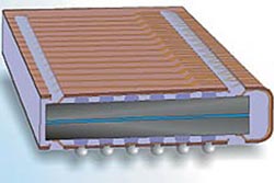
The memory chips are stacked on top of each other instead of being laid out side by side as they are today, thus maximizing the space on the motherboard. This will allow mobile phone manufacturers, MP3 players, and handheld devices to further reduce the size of their products.
In current multichip packages, different chips exist as independent “outposts,” separated by a protective barrier within the chip package. They communicate with each other and with other components through connecting wires to tiny metal balls that are soldered outside the barrier.
In contrast, the new chip package (tentatively called the wafer-level processed stack package, or WSP) utilizes a technology known as TSV (Through Silicon Vias). With TSV, a wire can run directly from the silicon circuit inside one chip to another chip. Therefore, less space is needed for barriers, connecting wires, and solder balls within the chip package.
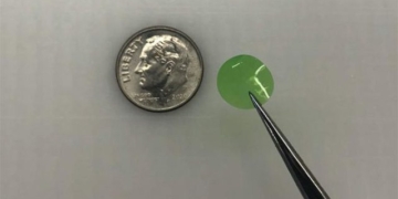
A Samsung chip package can contain up to 8 stacked chips. The sample product includes 8 2GB dynamic memory chips, resulting in a total capacity of 16GB within a height of only 0.56 mm. In the initial phase, the WSP will be applied only in dynamic memory cards.
In later phases, each WSP will be able to combine different types of chips. For example, a chip package could contain both DRAM and flash memory.
Thiên Ý


